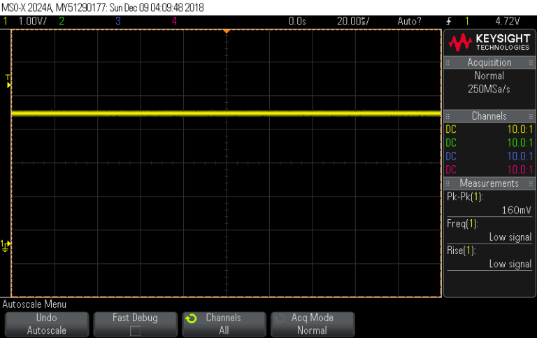
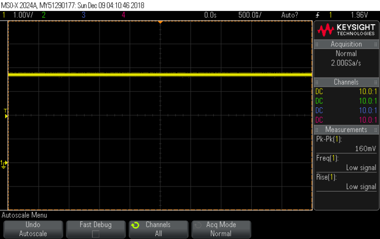
TS-430 Control Board: IC-1 Waveforms
TS-430 Control Board: IC-1 Waveforms
IC-1 is the main processor chip on the Control Board of the TS-430. It is a uPD8049c. This 40 pin chip runs at 5.74 Mhz, and interfaces with virtually every control integrated circuit (IC-2 through IC-6) on the board. You can see that it is central to the radio’s operation.


Pin 1: Data Selector Input – Receives button/switch status from IC-4 and IC-5.

Pins 2 & 3: Clock input – 5.74 MHz crystal oscillator


Pin 4: RESET

Pin 5 – Single Step – enables single stepping through program. Not used. Tied High.

Pin 6: INT – Interrupt Pin. Makes processor jump to a display update routine periodically, then return.

Pin 7: EA – External Access – Not Used. Tied to ground.

Pin 8: RD – Read Data Bus – Not Used.

Pin 9: PSEN – Program Store Enable Output. Not Used.
Pin 10: WR – Bus Write – Not Used.

Pin 11: ALE – Address Latch Enable output for external data or memory. Not used.

Pins 12 – 19: Bidirectional Data Bus. Used to exchange Mode Data with RAM and control circuits.
Pin 12: B0 – VFO “A” Indicator output

Pin 13: DB1 – VFO “B” Indicator output

Pin 14: DB2 – No memory signal output.

Pin 15: DB3 – MODE Output LSB
Pin 16: DB4 – MODE Output USB

Pin 17: DB5 – MODE Output CW

Pin 18: DB6 – MODE Output AM

Pin 19: DB7 – MODE Output FM

Pin 20: Ground

Pins 21-25: I/O Expander Control Output
Pin 21: P20 – Port 2 Bit 0

Pin 22: P21 Port 2 Bit 1

Pin 23: P22 – Port 2 Bit 2

Pin 24: P23 – Port 2 Bit 3

Pin 25: PROG – Clocks Instructions & Data to I/O Expander Chips IC-2 & IC-3.

Pin 26: Vdd +5 volts

Pin 27: P10 – Port 1 Bit 0 – TX Inhibit (Out of ham band)

Pin 28: P11 – Port 1 Bit 1 – Tx Inhibit – Out of ham & WARC Band

Pin 29: P12 – Pin 1 Bit 2 – 28 MHz Power Down Output

Pin 30: P13 – Port 1 Bit 3 – External Ram Control Output R/W to IC-6 Static Ram

Pin 31: P14 – Port 1 Bit 4 – P.SCAN Input

Pin 32: P15 – Port 1 Bit 5 – M.SCAN Input

Pin 33: P16 – Port 1 Bit 6 – FUNCTION Input

Pin 34: P17 – FUNCTION input M.CHAN Input

Pin 35: P24 – Port 2 Bit 4 – O/O Expander data selector control output

Pin 36: Port 2 Bit 5 – External RAM Control Output (CE) for IC-6

Pin 37: P26 – Port 2 Bit 6 – Encoder Up/Down Input

Pin 38: P27 – Port 2 Bit 7 – Voltage Down detection signal

Pin 39: T1 – Encoder Clock, P.SCAN clock input

Pin 40: VCC + 5 volts


Comments
Post a Comment