Receiver Noise Bridge – Pt 3
Receiver Noise Bridge – Pt 3
The articles I was basing this design on said that it was beneficial to isolate the variable resistor from the case, to reduce stray capacitance that affects the balance of the bridge. So I used a piece of perf board, and some metal standoffs that I had in the junk box. You can also see the beginnings of the bridge below. It is a trifiler wound transformer on a FT37-43 core. The fixed capacitor is about half the value of the variable cap. It is used to offset the variable cap approximately 1/2 range. That way, if the variable is on the lower half of the range, you are seeing an inductive reactance. If the variable cap is on the upper half (CW) of the range, you are reading capacitive reactance.
Here is the rest of the circuit. There is a 555 oscillator running at about 1kc, to modulate the noise generator. That makes it easier to tell when you tune to a null. The 555 drives a zener diode noise generator, which in turn drives a two-stage 2n3904 amplifier for the noise source. This noise is then applied to the bridge circuit. The trimmer is in place to balance out the stray capacitance in the circuit. There is a 1-turn “coil” in the unkown impedance input to the bridge. This is to balance out the stray inductance that shows up at higher frequencies.
Here is the top view…
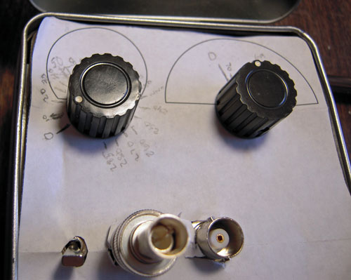
And here is the start of the calibration procedure. For the resistance scale, you just read the resistance of the variable pot, and transfer that read to the scale. For the reactance scale, I ended up using a 1/4 wave stub on 10 mhz, and calculated what the reactance would be at various frequencies. These reactance values were transferred to the reactance scale.
Continued Pt 4…


Comments
Post a Comment